User Manual
Updated: 16 December 2014, documenting firmware v1.9.
Copyright © 2008-2010 Thomas Pircher
This document is released under the terms of the Creative Commons Attribution-Share Alike 3.0 Unported License.
16 December 2014, v1.9.1
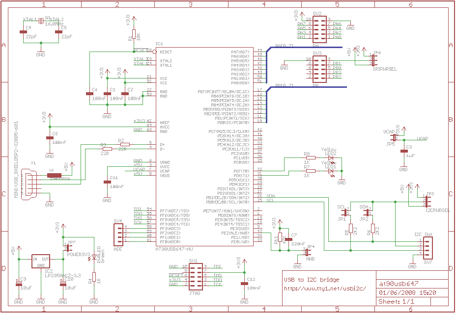
userial is an Open Source USB to I2C/SPI/GPIO bridge. The board uses an ATMEL AT90USB647 chip and provides the following interfaces:
1 × USB interface (serial emulation, to the PC)
1 × JTAG port
1 × I2C port
1 × SPI port
8 × General purpose digital I/O (GPIO) lines
4 × Analog to Digital (ADC) converters
The board communicates with the host computer using a CDC (USB communications device class).
This makes it easy to use userial without installing a device driver or special libraries.
Under Windows it is necessary to install a .inf file while Linux and Mac OS
will recognise the device correctly as serial port without particular configuration.
Due to the ASCII based command interface it is easy to control devices manually with just a terminal emulation.
This makes it easy to obtain quick results, to configure devices on-the-fly or to control prototyping boards in a straight-forward way.
Schematics and firmware are available to the public. The firmware is released under the terms of the MIT license and the hardware is released under the terms of the Creative Commons Attribution-Share Alike 3.0 Unported License.
userial is based on Dean Camera's LUFA (Lightweight USB Framework for AVRs) library.
The userial board is a USB communications device class (CDC) device and is visible as a virtual COM port to the user. Most Operating Systems already include drivers for this kind of device.
The serial settings are not important for the USB communication. The values of 115200 bps, 8 data bits, no parity, 1 stop bit are a safe choice. Hardware handshake should be turned off.
Virtually all UNIX systems include an ACM driver already in their kernel.
Under Linux this device is accessible as a /dev/ttyACMx device file.
The device can be opened using a serial terminal such as miniterm or cutecom.
The userial protocol is ASCII based, in order to make it easy to insert commands and to read the replies in a serial terminal emulation. In the following examples, lines starting with a less-than character (<) are commands sent to userial; lines with a greater-than character (>) are replies.
All commands are case insensitive, though the replies are always uppercase. It is possible to specify ASCII characters instead of hex numbers. Those characters must be escaped by a backslash.
A line must end with a carreage return '\r' or a newline '\n' or any combination of those two.
The software version can be queried with the 'V' command.
The only I2C configuration parameter so far is the clock rate. It is changed by using the 'I' command, followed by the 'C' character and the clock rate in kHz, expressed as a hexadecimal number. The reply to the configuration command is the clock rate effectively set in hardware.
To query the current configuration, just send the command 'IC'. The description of a I2C configuration command is:
IC[<dd>]
ICStart of a I2C configuration command.
<dd>The frequency of the I2C clock rate in kHz, expressed as a hexadecimal number.
The following example sets the I2C master clock frequency to 100kHz (0x64 in hexadecimal).
A complete I2C transaction is written entirely on one line. It starts with 'IS' (start) and ends with 'P' (stop) and may contain zero or more repeated start commands ('S') in between. The general form of a I2C read/write command is as follows:
IS<aa>(R|W)<dd>[S<aa>(R|W)<dd>…]P
ISI2C Start Command.
The reply to 'IS' is 'IS'.
<aa>The I2C slave address in a left-aligned form. The last bit of the address must match the Read/Write operation: 1 for a Read and 0 for a Write operation
The reply to '<aa>' is 'A' for an Acknowledge or 'N' for a Nack.
(R|W)One character, either 'R' or 'W' for a Read or a Write operation.
<dd>The operation payload of byte count. On a Read operation this number indicates the number of bytes to read from the slave. On a Write operation this is a sequence of hexadecimal 8-bit values: the payload to write to the slave.
The reply to a Write command is one 'A' for each byte written to the slave in case of success. If the slave Nacks one byte, the transaction will be stopped (a Stop condition is put on the bus) and a 'N' is sent to the user.
The reply to a Read command is the data read from the slave device.
SRepeated Start Condition. This command can be added to a command, resulting in a repeated start condition.
The reply to 'S' is always 'S'. This helps to distinguish between data bytes from different transactions.
PStop Condition.
The reply to 'P' is always 'P'.
In order to illustrate the command structure, let's write down a simple Read operation:
IS<aa>R<dd>P
and a simple Write operation:
IS<aa>W<dd>P
The following examples show the use of the commands.
Example 3.6. Combining write and read into one transaction
< IS12W010203S21R05P
> ISAAAASA3132333435P
If the data line (SDA) is stuck LOW, the master should send 9 clock pulses. The device that held the bus LOW should release it sometime within those 9 clocks.
In userial, this operation is currently implemented as Start condition, followed by a general call address and a Stop condition.
IX
IXThe I2C bus clear command. This command has no parameters. The reply to a 'IX' command is always IX.
The I2C specification defines a slave reset command. This reset consists of a General Call, followed by the byte 0x06. userial does not provide a specific command for it, because the following command can be used to achieve the same effect:
With the GPIO configuration command it is possible to specify the I/O direction of each pin of the I/O port individually.
GC<p><dddddddd>[<p><dddddddd>…]
GCStart of a GPIO configuration command.
<p>The port name. On the userial board, ports 'A' and 'B' are supported.
<dddddddd>The direction of the pins: 'I' for input or 'O' for output. The first character corresponds to bit 7, the last character corresponds to bit 0.
userial replies to a GPIO command with the configuration that has been actuated.
The following command configures the port B with pins 7,6,3,2 and inputs and pins 5,4,1,0 as outputs.
The read-back of ports is simple. The port names are listed after the 'GR' command. The data is returned in hexadecimal format.
GR<p>[<p>…]
GRStart of a GPIO read command.
<p>The port name.
userial replies to a GPIO command with the port number, followed by the logical value of the IO lines.
For example, to read port B and A back (in this order):
Individual bits can be set using the 'GB' command.
GB<p><dddddddd>[<p><dddddddd>…]
GBStart of a GPIO set command.
<p>The port name.
<dddddddd>The data of each pin: '1', '0', to set and reset a pin, 'F' to flip the value of a bit, 'X' to leave the value of a bit unchanged.
userial replies to a GPIO set command with the data read from the port, as a bit field.
For example, to write data to port A and B:
This command can also be used to read back the current value of a port, in a binary format:
The SPI configuration command can set a series of parameters: the operation mode, the data order and the clock frequency.
SC<m><o><dd>
SCStart of a SPI configuration command.
<m>The SPI mode. See Table 3.1 for possible values of this parameter.
Table 3.1. SPI mode
SPI Mode Shift SCK-edge Capture SCK-edge 0 Falling Rising 1 Rising Falling 2 Rising Falling 3 Falling Rising <o>When this value is set to 'L', the LSB of the data word is transmitted first. When this value is set to 'M', the MSB of the data word is transmitted first.
<dd>The frequency of the SPI clock rate in kHz, expressed as a hexadecimal number.
The reply to this command is the effective setting of the SPI interface.
Data are written to the SPI bus with the write command. It has the following form: the operation mode, the data order and the clock frequency.
SW[H|L]<dd>[<dd>…]
SWStart of a SPI transfer command.
[H|L]One optional character, either 'H' or 'L'. This parameter indicates if the SPI Slave Select line must be toggled during the transfer. If 'H', the SS line will be held high during the transfer, if 'L', the SS line will be held low. Specify nothing if the SS line should not be changed.
<dd>[<dd>…]One or more bytes of data to be written to the SPI slave.
The reply to this command is the data read during the transfer.
The ADC device can be configured to use the internal reference voltage, or one of the external voltages on AVcc or AREF. At startup, userial uses the internal reference, 2.56V.
To query the current configuration, send the command 'AC'. The description of a ADC configuration command is:
AC[<t><v.vv>]
ACADC config command.
<t>The type of voltage reference:
Table 3.2. ADC voltage reference type
Type Description 'I' Internal 2.56V Voltage Reference with external capacitor on AREF pin 'C' AVcc with external capacitor on AREF pin 'F' AREF, Internal Vref turned off <v.vv>The actual voltage reference. This value is used to calculate the voltage for the 'AV' command.
The reply to this command is the string "AC", followed by the ADC configuration.
The ADC peripheral can be used directly without initialisation. The only parameter the
AR<c>
ARStart of an ADC read command.
<c>The ADC channel.
The reply to this command is the string "AR", followed by the ADC value in headecimal format.
This command is actually the same as the previous ADC read command. The result is given as using the reference voltage given in the ADC config.
AV<c>
AVStart of an ADC Voltage read command.
<c>The ADC channel.
The reply to this command is the string "AV", followed by the voltage in decimal.
The userial firmware is pre-compiled for the ATMEL AT90USB647 chip. The software can be compiled using AVR-GCC under Linux, *BSD and Mac OS, or WinAVR under Windows. Just type make on the command line prompt.
Alternative target or frequency can conveniently be set by overriding the MCU and F_CPU
variables in the project Makefile.
Alternatively, the variables can be specified on the command line, as in the following example:
make MCU=at90usb162 F_CPU=8000000UL
The file version.h allows to selectively disable some features in the firmware.
These compile switched all start with the prefix FEATURE_.
A value of 1 enables the feature, a 0 disables it.
ATMEL ships the chip with a pre-programmed boot loader. This makes it possible to update the userial firmware with just a USB cable. All that's needed is a USB cable, a jumper and ATMEL's FLIP boot loader. Follow this list for an update of the firmware:
Power down the userial board
Close the jumper JP4
Power up the userial board by connecting it to the PC
Launch FLIP boot loader and update the firmware
Power down the userial board
Remove jumper JP4
An alternative to FLIP, especially for Linux and OS X is dfu-programmer.
Since ATMEL's FLIP boot loader is not Open Source and the protocol is not published, people have written alternative boot loaders. One very good boot loader is Dean Camera's ButtLoad, that is also included in the LUFA library. This boot loader uses a protocol documented in the application note AVR109: Self Programming.
Firmware upgrades are performed as in the section called “Firmware upgrade using FLIP”, with the only variation in the download procedure. The following example used avrdude to download the firmware, but alternative clients, include AVR Studio, can be used instead.
avrdude -p at90usb647 -P /dev/ttyACM0 -c avr109 -U flash:w:userial.hex
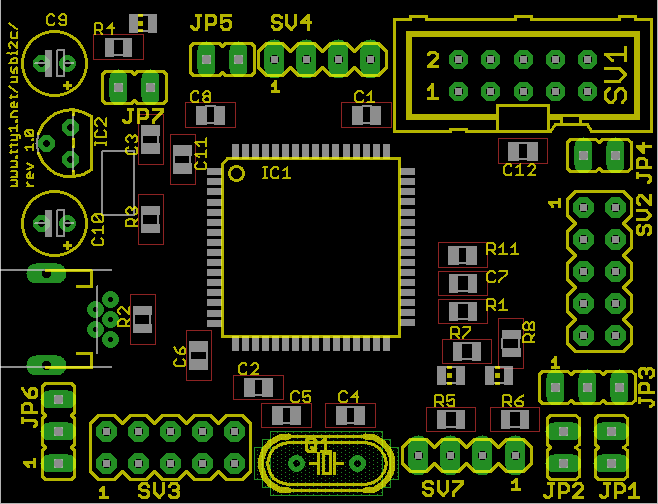
Table 5.1. Jumpers
| Jumper | Position | Default | Function |
|---|---|---|---|
| JP1 | C5 | closed | Pull-up resistor on SCL line. If open, the pull-up resistor is disconnected. |
| JP2 | C5 | closed | Pull-up resistor on SDA line. If open, the pull-up resistor is disconnected. |
| JP3 | C6 | 1-2 closed | Power selector for SCL and SDA pull-ups. In position 1-2 the pull-ups are connected to +3V3, in position 2-3 the pull-ups are connected to +5V. If no jumper is set, both pull-ups are disabled. |
| JP4 | D5 | open | Boot loader enable. When this jumper is closed the controller runs the boot loader code instead of the application code. Used for firmware upgrades. |
| JP5 | B6 | open | For testing purposes. If closed, the AVR micro will source power to the circuit. This jumper must be left open all the time. |
| JP6 | A6 | 1-2 closed | Power selector for SPI interface. In position 1-2 the SPI power is +3V3, in position 2-3 the power is +5V. |
| JP7 | D1 | closed | Power switch. When this jumper is open the micro controller is disconnected from the power supply. |